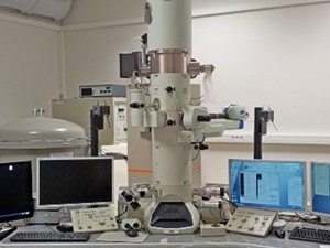
- Accelerating voltage: 200 kV
- Resolution: 0.23 nm
- Specimen holders: single tilt, dual analytical tilt
- 2 Gatan 2K cameras
- STEM BF/HAADF
Local chemical analysis using BF/HAADF and EDX STEM is possible thanks to a small probe (0.2 to 1.5 nm).
- JEOL Centurio 1 mrad EDX Detector
- ACOM - ASTAR Orientation Mapping
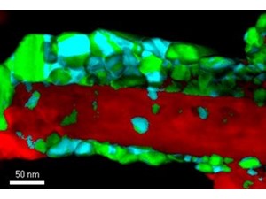
Special feature: Implementation of ASTAR, the trade name for the Automated Crystal Orientation Mapping (ACOM) technique.
The technique is similar to EBSD as used in SEMs, but involves applying an electron beam (probe <=2 nm) to a thin section for TEM. The diffraction patterns obtained over an area of a few µm² are compared to user-defined databases to generate orientation and phase maps.
Visualization of two phases of CdSe (cubic in blue, hexagonal in green) around a ZnO nanowire (red) using ASTAR
Benefits:
- Small-sized probe enabling grain orientation measurement for grains < 10 nm
- Not sensitive to material deformation or surface oxidation
- Use of precession to improve orientation measurement quality.
Disadvantage:
- The analyzed area is relatively small (max. 10x10 µm)
* CEMAM investment in 2013, coll. Institut Carnot "Energies du futur", Isterre-UJF, Nanomegas, SIMAP
Reserve equipment
Sponsored by
The French National Research Agency