
The current surge in demand for structured materials—such as those used in microelectronics—and for energy harvesting technologies calls for the development of increasingly sophisticated characterization tools. With this in mind, a nanoindenter that can be used in situ within a scanning electron microscope (SEM) is currently being developed.
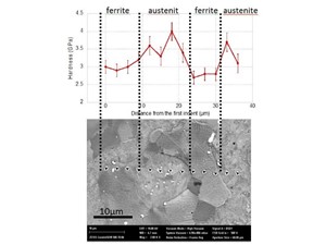
Nanoindentation is a powerful technique for characterizing local mechanical properties. In nanoindentation, the probed depth range extends from a few nanometers to a micrometer, enabling the study of thin films or submicrometer-scale objects. Based on load, displacement, and contact stiffness data, hardness and Young’s modulus can be calculated continuously. Furthermore, numerical post-processing using the finite element method enables the identification of mechanical behavior laws (e.g., stress-strain curves).
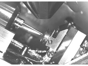
The in-situ nanoindentation setup with SEM allows for precise positioning of measurements on sub-micrometer-scale objects (resolution < 100 nm) and real-time imaging of mechanical events that may occur during indentation
The integration of nanoindentation with EDS and EBSD techniques is currently under development.
The nanoindentation head is also compatible with high-resolution electrical measurements during testing.